CIRCUIT INTÉGRÉ
Référence: TLP 561-G
Disponibilité: En Stock
Circuit intégré
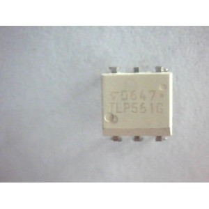
TLP561G
1 2002-09-25
TOSHIBA Photocoupler GaAs Ired & Photo?Triac
TLP561G
Triac Driver
Programmable Controllers
AC?Output Module
Solid State Relay
The TOSHIBA TLP561G consists of a zero voltage crossing turn?on
photo?triac optically coupled to a gallium arsenide infrared emitting
diode in a six lead plastic DIP package.
�� Peak off?state voltage: 400V(min.)
�� On?state current: 100mA(max.)
�� Isolation voltage: 2500Vrms(min.)
�� UL recognized: file no. E67349
�� Isolation operating voltage: 2500Vac or 300Vdc for isolation
groupe C*1
�� Trigger LED current
Trigger LED Current (mA)
Classi VT = 6V, Ta = 25°C �
fication* Min. Max.
Marking Of
Classification
(IFT5) ? 5 T5
(IFT7) ? 7 T5, T7
Standard ? 10 T5, T7, blank
*Ex. (IFT5); TLP561G (IFT5)
(Note) Application type name for certification test, please
use standard product type name, i.e.
TLP561G (IFT5): TLP561G
*1: According to VDE0110, table 4.
Pin Configuration (top view)
1 : ANODE
2 : CATHODE
3 : N.C.
4 : TERMINAL 1
6 : TERMINAL 2
1
2
4
6
3 ZC
Unit in mm
TOSHIBA 11?7A9
Weight: 0.39g
TLP561G
2 2002-09-25
Maximum Ratings (Ta = 25°C)
Characteristic Symbol Rating Unit
Forward current IF 50 mA
Forward current derating (Ta ? 53°C) ?IF / °C �0.7 mA / °C
Peak forward current (100?s pulse, 100pps) IFP 1 A
Reverse voltage VR 5 V
LED
Junction temperature Tj 125 °C
Off�state ontput terminal voltage VDRM 400 V
Ta = 25°C 100
On�state RMS current
Ta = 70°C
IT(RMS)
50
mA
On�state current derating (Ta ? 25°C) ?IT / °C �1.1 mA / °C
Peak on�state current (100?s pulse, 120pps) ITP 2 A
Peak nonrepetitive surge current
(Pw = 10ms, DC = 10%) ITSM 1.2 A
Detector
Junction temperature Tj 115 °C
Storage temperature range Tstg �55~125 °C
Operating temperature range Topr �40~100 °C
Lead soldering temperature (10s) Tsol 260 °C
Isolation voltage (AC, 1 min., R.H. ? 60%) BVS 2500 Vrms
Recommended Operating Conditions
Characteristic Symbol Min. Typ. Max. Unit
Supply voltage VAC ?� ? 120 Vac
Forward current IF 15 20 25 mA
Peak on�state current ITP ?� ?� 1 A
Operating temperature Topr �25 ? 85 °C
TLP561G
3 2002-09-25
Individual Electrical Characteristics (Ta = 25°C)
Characteristic Symbol Test Condition Min. Typ. Max. Unit
Forward voltage VF IF = 10mA 1.0 1.15 1.3 V
Reverse current IR VR = 5V ? ? 10 ?A
LED
Capacitance CT V = 0, f = 1MHz ? 30 ? pF
Peak off�state current IDRM VDRM = 400V ? 10 100 nA
Peak on�state voltage VTM ITM = 100mA ? 1.7 3.0 V
Holding current IH ? ? 0.6 ? mA
Critical rate of rise of
off�state voltage dv / dt Vin = 120Vrms, Ta = 85°C
(Fig.1) 200 500 ? V / ?s
Detector
Critical rate or rise of
commutating voltage dv / dt (c) Vin = 30Vrms, IT = 15mA
(Fig.1) ? 0.2 ? V / ?s
Coupled Electrical Characteristics (Ta = 25°C)
Characteristic Symbol Test Condition Min. Typ. Max. Unit
Trigger LED current IFT VT = 3V, RL = 100? ? 5 10 mA
Inhibit voltage VIH IF = rated IFT ? ? 40 V
Leakage in inhibited state IIH IF = rated IFT
VT = rated VDRM ? 100 300 ?A
Capacitance
(input to output) CS VS = 0, f = 1MHz ? 0.8 ? pF
Isolation resistance RS VS = 500V 5×10¹⁰ 1014 ? ?
AC, 1 minute 2500 ? ?
AC, 1 second, in oil ? 5000 ?
Vrms
Isolation voltage BVS
DC, 1 minute, in oil ? 5000 ? Vdc
Fig.1: dv / dt test circuit
dv / dt
( )
dv / dt
5V, VCC
0V
1
2
3
6
4
Rin
4k?
VCC 120?
Vin
–
+
RL
TLP561G
4 2002-09-25
Ambient temperature Ta (°C)
IF – Ta
Allowable forward current
IF (mA)
–20 0 20 40 60 80 100 120
100
80
0
60
40
20
Ambient temperature Ta (°C)
120
IT(RMS) – Ta
R. M. S. On-state current
IT (RMS) (mA)
–20 0 20 40 60 80 100
200
160
0
120
80
40
Duty cycle ratio DR
IFP – DR
Allowable pulse forward current
IFP (mA)
3 10-3 3 3
3000
10
1000
500
30
100
50
300
10-2 10-1 3
Pulse width ≦ 100?s
Ta = 25°C
100
IF – VF
Forward current IF (mA)
Forward voltage VF (V)
100
50
0.3
5
0.5
30
3
1
10
0.1
0.6 0.8 1.0 1.2 1.4 1.6 1.8
Ta = 25°C
?VF/?Ta – IF
Forward voltage temperature
coefficient ?VF/?Ta (mV/°C)
–3.2
–2.0
–2.4
–2.8
–0.4
–1.6
–1.2
–0.8
Forward current IF (mA)
0.1 0.3 0.5 1 3 5 10 30 50
IFP – VFP
Pulse forward current IFP (mA)
Pulse forward voltage VFP (V)
1000
500
0.6
3
50
5
300
30
10
100
1
1.0 1.4 1.8 2.2 2.6
Pulse width≦10?s
Repetitive
Frequency = 100Hz
Ta = 25?
TLP561G
5 2002-09-25
–20 0 20 40 60 80 100
3
1.2
1
0.5
0.3
0.1
–40
2
Ambient temperature Ta (?)
Holding current IH
(arbitrary unit)
Normalized IH – Ta
Ambient temperature Ta (?)
Trigger LED current IFT
(arbitrary unit)
Normalized IFT – Ta
VT = 3V
–20 0 20 40 60 80 100
3
1.2
1
0.5
0.3
0.1
–40
2
Normalized IDRM – Ta
Ambient temperature Ta (?)
103
0 20 40 60 80
Peak off-state current IDRM
(arbitrary unit)
100
102
101
100
VDRM = Rated
Ambient temperature Ta (?)
Off-state output terminal voltage
VDRM (arbitrary unit)
Normalized VDRM – Ta
1.4
–40 0 80 100
1.2
1.0
0.8
0.6
0.4
0.2
–20 20 40 60
Inhibit voltage VIH
(arbitrary unit)
–20 0 20 40 60 80 100
3
1.2
1
0.5
0.3
0.1
–40
2
Ambient temperature Ta (?)
Normalized VIH – Ta
IF = Rated IFT
Inhibit current IIH
(arbitrary unit)
–20 0 20 40 60 80 100
3
1.2
1
0.5
0.3
0.1
–40
2
Ambient temperature Ta (?)
Normalized IIH – Ta
IF = Rated IFT
VT = Rated VDRM
TLP561G
6 2002-09-25
�� TOSHIBA is continually working to improve the quality and reliability of its products. Nevertheless, semiconductor
devices in general can malfunction or fail due to their inherent electrical sensitivity and vulnerability to physical
stress. It is the responsibility of the buyer, when utilizing TOSHIBA products, to comply with the standards of
safety in making a safe design for the entire system, and to avoid situations in which a malfunction or failure of
such TOSHIBA products could cause loss of human life, bodily injury or damage to property.
In developing your designs, please ensure that TOSHIBA products are used within specified operating ranges as
set forth in the most recent TOSHIBA products specifications. Also, please keep in mind the precautions and
conditions set forth in the “Handling Guide for Semiconductor Devices,” or “TOSHIBA Semiconductor Reliability
Handbook” etc..
�� The TOSHIBA products listed in this document are intended for usage in general electronics applications
(computer, personal equipment, office equipment, measuring equipment, industrial robotics, domestic appliances,
etc.). These TOSHIBA products are neither intended nor warranted for usage in equipment that requires
extraordinarily high quality and/or reliability or a malfunction or failure of which may cause loss of human life or
bodily injury (“Unintended Usage”). Unintended Usage include atomic energy control instruments, airplane or
spaceship instruments, transportation instruments, traffic signal instruments, combustion control instruments,
medical instruments, all types of safety devices, etc.. Unintended Usage of TOSHIBA products listed in this
document shall be made at the customer’s own risk.
�� Gallium arsenide (GaAs) is a substance used in the products described in this document. GaAs dust and fumes
are toxic. Do not break, cut or pulverize the product, or use chemicals to dissolve them. When disposing of the
products, follow the appropriate regulations. Do not dispose of the products with other industrial waste or with
domestic garbage.
�� The products described in this document are subject to the foreign exchange and foreign trade laws.
�� The information contained herein is presented only as a guide for the applications of our products. No
responsibility is assumed by TOSHIBA CORPORATION for any infringements of intellectual property or other
rights of the third parties which may result from its use. No license is granted by implication or otherwise under
any intellectual property or other rights of TOSHIBA CORPORATION or others.
�� The information contained herein is subject to change without notice.
000707EBC RESTRICTIONS ON PRODUCT USE
Triac Driver
Programmable Controllers
AC?Output Module
Solid State Relay